Manufactured in Greater NoidaGenuine Philips UV-C LampsIIT Patna Alumni on Our TeamExporting to 20+ Countries

Electronics and semiconductor manufacturing require ultrapure water (UPW) with resistivity approaching the thermodynamic limit (18.2 MΩ·cm), total organic carbon below 5 ppb, and bacteria counts below 0.1 CFU/mL — the most demanding water quality specifications in any industrial application. UV disinfection at 185+254 nm is a standard, indispensable component of every UPW production system: 254 nm UV inactivates microorganisms with 4-log efficiency, while 185 nm (vacuum UV) generates hydroxyl radicals that photo-oxidise dissolved organics, reducing TOC by 50–80% in a single pass. Alpha UV System supplies SEMI F63-aligned dual-wavelength UV units for Indian PCB manufacturers, LED/lighting fabs, solar PV plants, and the emerging semiconductor fabrication sector.
UV Dose
40–200 mJ/cm²
Capacity
500 – 20,000 LPH
The electronics manufacturing industry demands the purest water of any industrial sector. In printed circuit board fabrication, LED and photovoltaic wafer production, and semiconductor manufacturing, water contacts device surfaces at critical process steps — wafer rinsing after etching, chemical-mechanical planarization (CMP), photoresist stripping, copper electroplating rinses, and final clean before packaging. Any contaminant in the process water — a bacteria cell, an organic molecule, a metal ion, a sub-micron particle — can deposit on the device surface, causing a structural defect that reduces product yield.
The economic stakes are severe. In advanced PCB manufacturing, a 1% reduction in yield on a production line processing 10,000 boards per day at ₹500 per board represents a ₹50 lakh per day loss. In solar PV cell manufacturing, UPW contamination causing surface defects that reduce cell efficiency by 0.1% (absolute) on 1 MW per day production represents thousands of rupees per day in reduced panel value over product lifetime. Investing in a UV system that costs ₹2–10 lakh and prevents these yield losses is the simplest capital allocation decision in the electronics plant.
SEMI F63-0304 (Guide for Ultrapure Water Used in Semiconductor Processing) and ASTM D5127 (Standard Guide for Ultra-Pure Water Used in the Electronics and Semiconductor Industry) define the quality specifications that Indian electronics manufacturers must meet. The Indian electronics manufacturing sector, while primarily producing PCBs, LEDs, solar cells, and consumer electronics rather than advanced logic semiconductor, requires UPW at the lower-to-middle tier of SEMI F63 — TOC <20 ppb, resistivity ≥15 MΩ·cm, and bacteria <1 CFU/mL for PCB and LED applications. UV is the critical technology for achieving both the TOC and bacteria specifications simultaneously.
Total organic carbon in UPW originates from several sources that RO membranes do not completely eliminate: dissolved CO₂ converting to carbonic acid (managed by degassing), residual organic compounds in RO permeate (typically 30–60 ppb after good pre-treatment), and organics leached from ion-exchange resin beads and PVDF distribution piping — even PVDF, the most inert of engineering polymers, leaches trace organics into ultra-pure water over time.
The photochemical mechanism of 185 nm UV for TOC reduction is well-established in the literature on advanced oxidation processes (Oppenlander, Photochemical Purification of Water and Air, Wiley-VCH, 2003; Semiat, Water International, 2008). When 185 nm photons are absorbed by water molecules, they photodissociate water into hydrogen atoms (H•) and hydroxyl radicals (OH•). The hydroxyl radical is among the most powerful oxidising species in aqueous chemistry, attacking dissolved organic molecules through hydrogen abstraction and addition, converting organic carbon chains to CO₂ and water in multi-step radical chain reactions. The ionic CO₂ produced temporarily appears as dissolved inorganic carbon (DIC) and carbonic acid, slightly increasing conductivity immediately after the UV chamber — but downstream mixed-bed DI or EDI removes both the CO₂ and the organic acid products, restoring full resistivity and reducing TOC to below 2 ppb in the final UPW.
The UPW production system for an Indian electronics manufacturing facility typically follows this sequence: raw water → pre-treatment (multimedia filter, activated carbon) → RO (primary TOC and bacteria reduction) → UV + degasser → mixed-bed DI or EDI → UPW storage tank → distribution loop (with UV on loop return) → point-of-use tool connections.
UV in the primary position (after RO, before mixed-bed DI) serves dual purposes: 185 nm photo-oxidation of TOC to ionic products that the downstream DI removes, and 254 nm inactivation of the trace bacteria (10–100 CFU/mL) that pass through the RO membrane. In this position, the UV system processes water with relatively low initial TOC (30–60 ppb from RO), which is the most efficient regime for 185 nm TOC reduction.
UV on the distribution loop return (254 nm) prevents bacterial regrowth in the loop during low-demand periods — nights, weekends, and production shutdowns when loop velocities fall and bacteria in biofilm pockets can multiply. This is critical: without loop UV, UPW systems that are bacteriologically clean at start-of-shift can accumulate bacterial counts exceeding SEMI F63 limits within 4–6 hours of low-flow operation. For multi-building electronics complexes with long distribution loop runs, multiple UV units on different loop segments may be specified to ensure uniform bacterial control throughout the loop.
Some high-purity water systems in advanced semiconductor manufacturing use dissolved ozone as the primary organic carbon removal agent, because ozone provides very high hydroxyl radical yield when combined with UV or hydrogen peroxide. However, dissolved ozone must be completely eliminated before the water contacts semiconductor devices — ozone at the ppb level oxidises silicon surfaces and interferes with thin-film deposition processes critical to semiconductor fabrication.
UV at 254 nm is the most effective and controllable method for ozone destruction in UPW. The photo-absorption cross-section of ozone at 254 nm is high, allowing complete ozone decomposition (O₃ → O₂) at UV doses well below those needed for microbial disinfection. In UPW systems using ozone, the process sequence is: RO permeate → ozone injection → ozone contact chamber → 254 nm UV for ozone destruction → mixed-bed DI → UPW distribution. Alpha UV System can supply UV units specified for ozone service — ozone-compatible EPDM or PTFE seals, chamber materials rated for continuous ozone exposure at 0.5–5 mg/L dissolved ozone, and quartz sleeves with confirmed stability in ozone-containing water.
The relationship between UV dose (at 185 nm) and TOC reduction in UPW follows an approximately logarithmic relationship: increasing dose provides diminishing returns as the most reactive organic fractions are oxidised first, with more recalcitrant organics requiring higher doses. Published data from the Ultrapure Water journal and SEMI technical publications indicate that for typical RO permeate with TOC of 30–50 ppb, 185+254 nm UV at 80–100 mJ/cm² (at 185 nm) achieves 70–80% TOC reduction, bringing outlet TOC to 6–15 ppb before downstream DI polishing.
Combined with the subsequent mixed-bed DI or EDI stage, which removes the ionic CO₂ and residual organic acid products of photo-oxidation and provides final resistivity polish, total TOC in the UPW distribution loop can be maintained below 2–5 ppb for PCB/LED applications (SEMI F63 Tier 2) and below 1 ppb for advanced semiconductor applications (Tier 3) with appropriate UV dose and DI capacity.
The ITRS (International Technology Roadmap for Semiconductors, 2015 Edition) confirms that TOC control in UPW is one of the most critical yield-enabling factors at sub-28 nm semiconductor process nodes, with TOC limits becoming progressively tighter as device feature sizes shrink and surface-area-to-volume ratios increase.
A common concern among electronics manufacturing engineers first evaluating UV for UPW applications is whether UV treatment will degrade the resistivity of their ultra-pure water. This concern is well-founded for 185 nm UV specifically, because the ionic products of photo-oxidation (dissolved CO₂, organic acids) do temporarily increase the ionic content of the water immediately after the UV chamber.
However, this is manageable through correct system design: the 185 nm UV unit must be positioned upstream of the mixed-bed DI or EDI polishing stage, not downstream. When UV is correctly positioned upstream of the final polishing stage, all ionic products of photo-oxidation are removed by the DI/EDI before the water enters the distribution loop. The net result is UPW with both lower TOC and full resistivity (17.5–18.2 MΩ·cm achievable after UV + EDI). At 254 nm only (no 185 nm), there is zero effect on resistivity at any dose used in water treatment — 254 nm acts only on microbial DNA and has no photo-oxidation effect on dissolved ions or organic molecules.
ASTM D5391 (Standard Test Method for Electrical Conductivity and Resistivity of a Flowing High-Purity Water Sample) provides the measurement protocol for confirming resistivity compliance in UPW distribution systems. Alpha UV System provides resistivity test data from UV installations on request, confirming that UV systems are correctly positioned and operating without negative impact on UPW conductivity specifications.
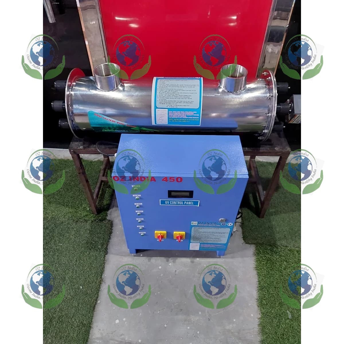
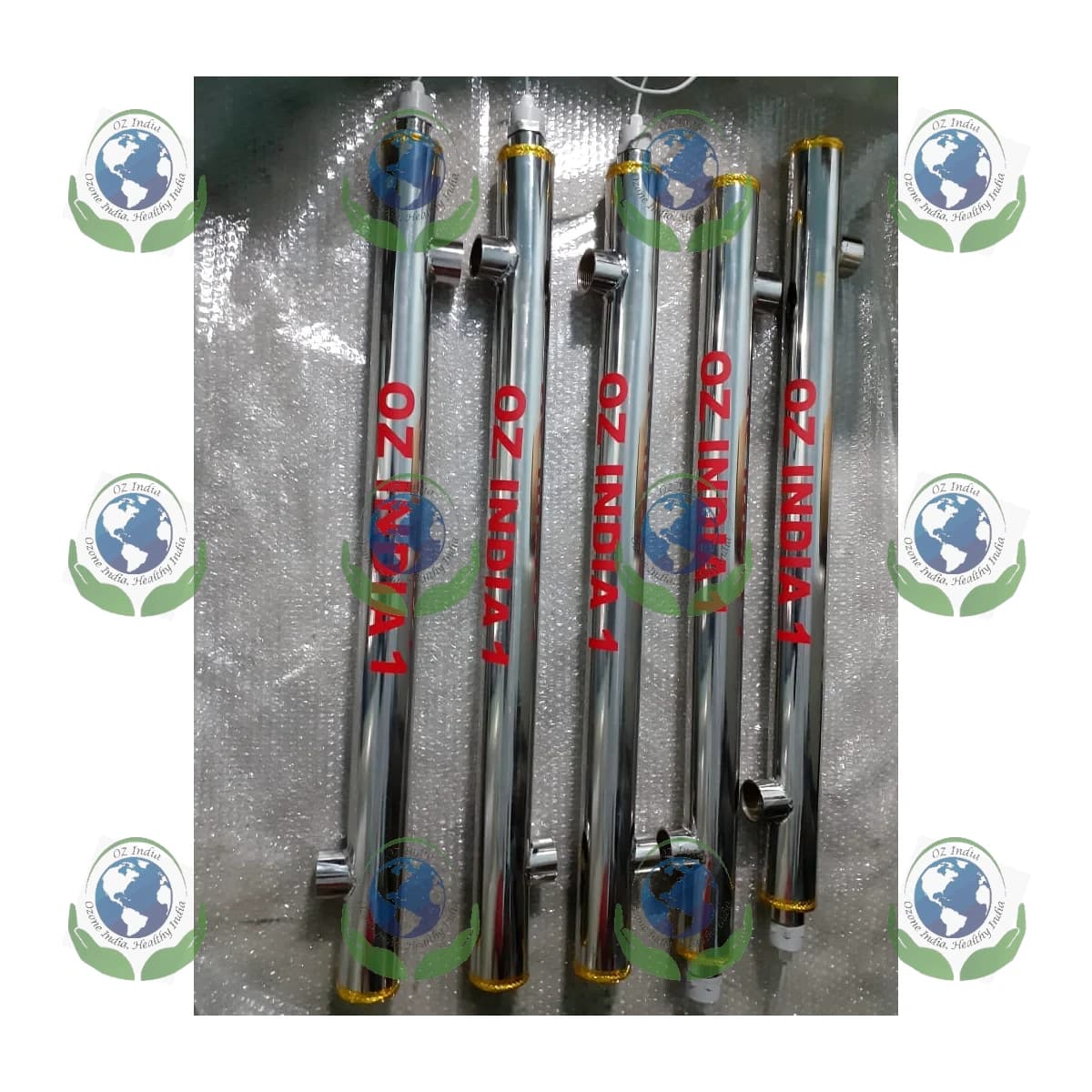
The extreme purity requirements of UPW create demanding material specifications for UV systems. Any material in contact with UPW that leaches organic compounds or metallic ions will contaminate the water and may cause wafer defects. Standard industrial UV materials — copper wire insulation, chrome-plated fittings, NBR seals, ABS polymer housings — are incompatible with electronics-grade UPW service.
Alpha UV System's electronics-grade UV units meet the following specifications:
Chamber Body: 316L stainless steel, electropolished to Ra <0.4 µm on wetted surfaces (reducing surface area for organic adsorption and biofilm attachment).
Wetted Polymer Parts: USP Class VI PTFE or PVDF throughout — fittings, valve bodies, o-rings, lamp holders. PTFE and PVDF have the lowest organic leachable profiles of any commercially available engineering polymers.
Quartz Sleeves: Synthetic fused silica (equivalent to GE Spectrosil 2000 or Heraeus Suprasil) for maximum 185 nm transmission (>80% at 185 nm). Standard quartz transmits negligibly at 185 nm and is not suitable for TOC-reduction applications.
Lamp Holders: High-purity alumina ceramic (99.5% Al₂O₃) for zero metallic extractables.
Pre-delivery Cleaning: UV chambers assembled in controlled environment, flushed with Type I reagent water (ASTM D1193) and TOC-certified to confirm <5 ppb TOC extractable from the unit before delivery.
India's National Electronics Policy (NEP 2019) and the PLI (Production Linked Incentive) scheme for electronics manufacturing have catalysed rapid expansion of PCB manufacturing, LED production, solar PV module manufacturing, and consumer electronics assembly across clusters in Bengaluru, Pune, Noida, Hosur, Chennai, and Rajasthan. Each of these sectors requires high-purity or ultra-pure water, and India's growing semiconductor ambitions (with planned fabrication facilities in Gujarat and Assam) will require SEMI F63 Tier 3 UPW systems at scales not previously seen in Indian industry.
Alpha UV System's IIT Patna-trained engineers are positioned to support India's electronics manufacturing expansion with UV systems correctly specified for each application tier — from 254 nm bacterial control for consumer electronics assembly rinse water through to dual-wavelength 185+254 nm TOC + bacteria control for PCB and solar PV, and full SEMI F63-aligned systems for planned semiconductor fabrication. Contact us via WhatsApp 9318305878 for electronics manufacturing UV specifications, with 24–48 hour response on technical enquiries.
Recommended Products
IIT Patna engineers recommend these systems for electronics uv applications based on flow rate, required UV dose, and compliance standard. Both systems use genuine Philips UV-C lamps and ship with complete compliance documentation.
High-flow UV water treatment for pharmaceutical WFI, food & beverage process water, and industrial applications. Revised Schedule M 2025, HACCP, and FSSAI compliant. IQ/OQ/PQ documentation.
UV water disinfection for hotels, restaurants, offices, and educational institutions. HACCP and FSSAI compliant documentation. Trusted by Taj Hotels, McDonald's India, and IIT Kanpur.
IIT Patna Engineering
Alpha UV System IIT Patna engineers calculate UV dose from your actual water quality parameters — measured UVT, flow rate, target log reduction, and the specific compliance standard that governs your facility. Not from catalogue sizing tables or generic assumptions. Every system ships with a signed UV dose calculation report, a Philips certificate of authenticity, and compliance documentation prepared for the regulatory framework applicable to electronics uv operations.
From measured UVT, flow rate, and target log-reduction. Signed by IIT Patna engineer.
SEMI F63 · ITRS Roadmap · ASTM D5391 · ISO 14644 — documentation prepared to the audit checklist, not generic templates.
WhatsApp your flow rate, water quality, and compliance requirement — engineering-backed quote in 2 hours.
Mon–Sat · 9 AM–6 PM IST · IIT Patna alumni on call
Send us your flow rate and compliance requirement — quote with engineering rationale in 2 hours.
+91 93183 05878
Get Quote →
Call Direct
+91 95995 00580
Tap to Call →
Send Enquiry
Detailed specifications form
Open Form →